







Unlocking the Power of Customized PCB Design
2025-03-16
Customized PCB design has become an integral aspect of electronic development, allowing engineers and designers to create tailored solutions that meet the unique requirements of their projects. The process involves several key steps and considerations, ensuring that the final product is functional, reliable, and optimized for performance.
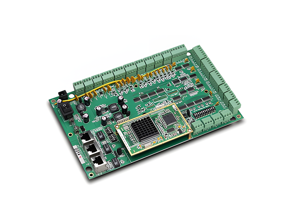
One of the primary benefits of customizing PCB design is the ability to tailor the layout and specifications to meet specific application requirements. This customization can include adjustments in size, shape, and component placement, which are crucial for fitting into unique enclosures or adhering to space constraints. By optimizing these factors, designers can enhance the overall efficiency and functionality of their electronic devices.
Another significant advantage lies in the ability to select materials and technologies that best suit the intended use of the PCB. For instance, high-frequency applications may require specific substrates to minimize signal loss, while industrial applications might prioritize durability and resistance to environmental factors. Customizing PCB design allows engineers to choose the right materials that enhance performance and longevity.
The design process typically begins with the creation of a schematic, which outlines the electrical connections and components. Once the schematic is approved, designers use specialized software to develop the physical layout of the PCB. This software enables designers to visualize the board and make necessary adjustments before moving to production. During this phase, it is crucial to consider factors such as trace width, spacing, and layer count, as these elements significantly impact the board's performance and manufacturability.
After finalizing the design, a prototype is often created to test the functionality of the PCB. This step is essential for identifying any potential issues and ensuring that the design meets all electrical and mechanical requirements. Once the prototype is validated, the board can move into full production.
It's also worth noting that the trend towards smaller and more complex electronic devices has increased the demand for advanced PCB designs. Techniques such as multi-layer PCBs and embedded components are becoming more prevalent, allowing for greater functionality in smaller footprints. By leveraging these techniques in customized PCB design, manufacturers can create innovative products that push the boundaries of technology.
In conclusion, customized PCB design is a vital process in the electronics industry, offering numerous benefits in terms of performance, efficiency, and adaptability. By understanding the intricacies of this process, engineers and designers can create exceptional products tailored to meet specific needs, ultimately propelling innovation in the field of electronics.
Related news


Request A Quote
Please feel free to contact us at any time, and we will wholeheartedly provide you with the highest quality service and support.
Copyright © 2022-2026 Shenzhen One Stone Two Birds Technology Co.,Ltd
Power by 300.cn